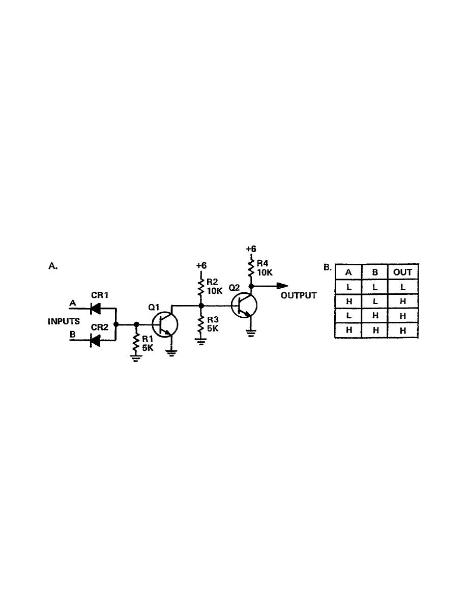
c. Current from ground to +6 volts establishes a voltage of +2 volts at the junction of R2 and
R3, due to the voltage drop across R3. The +2 volts is applied to the base of Q2.
d. Q2 is also an NPN transistor. A positive voltage on the base with respect to the emitter
causes Q2 to conduct heavily. The transistor conducts at saturation or maximum current. Current
through it would not increase even if we increased the positive voltage on its base.
e. The current path is from ground, through Q2 and R4, to the +6 volt supply. A transistor in
saturation offers so little resistance to current that we can consider its resistance zero, and all of the
voltage is dropped across R4. The collector of Q2, and, therefore, the output, is at 0 volts.
f. You can think of the operation of transistors in binary circuits as if they were switches. Their
condition is normally either cutoff or saturation, similar to a switch when it is open or closed. When a
switch is open (cutoff), there is no current. When the switch is closed (saturation), it has no resistance.
g. Looking at the circuit in A, Figure 3-3, we have found that with all inputs at 0 the output is 0.
This fact proves the circuit is an OR gate for at least one condition.
Figure 3-3. Transistorized positive OR circuit
10.
Using highs and lows on the OR circuit for the condition we completed above, we would apply
the high (H) designation to the +6 volt level and the low (L) designation to the 0 volt level. Looking
again at the OR circuit in Figure 3-3 for the condition we've already discussed, we can say that with all
lows (0 volt inputs) the circuit provides a low output. We've listed this in the first line of the truth table
in B, Figure 3-3. In binary designation this is the same as saying that all binary 0s in cause a binary 0
out.
11.
Now let's reexamine the schematic in A, Figure 3-3, with different input conditions. Assume
that input A changes from 0 volts (L) to +6 volts (H).
20


 Previous Page
