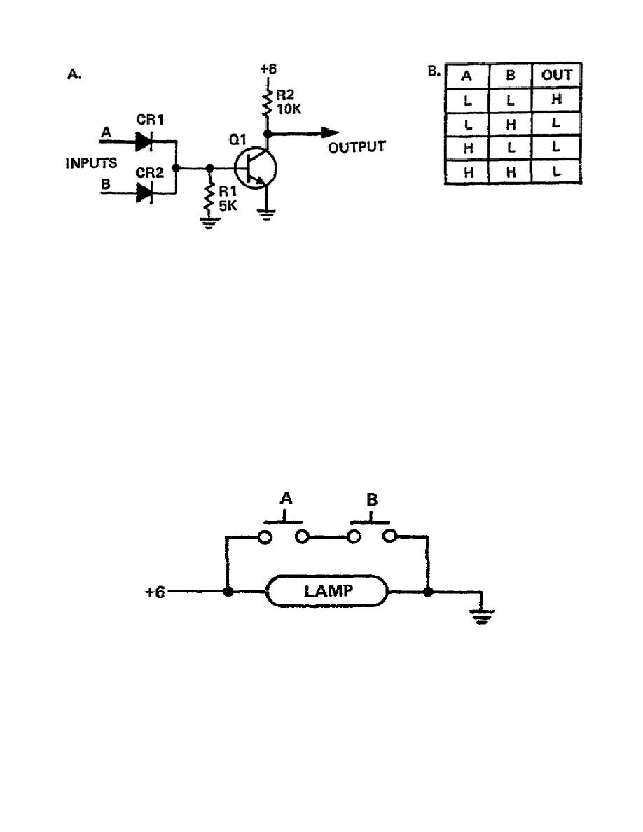
Figure 3-10. Transistorized positive NOR circuit
3.
A NAND gate output is high when any one or more inputs are low or NOT ANDed. When all
inputs are on, the NAND gate output is off. Charging this to voltage levels and considering only
positive logic, we can say that a NAND gate output is high (binary 1) when any input is low (binary 0).
Also, when all inputs are high the output is low.
4.
The switches and lamp circuit can be arranged as shown in Figure 3-11 so that it follows the
rules below. Here again, it is assumed that there is a resistor between the +6 VDC input and the power
supply that would prevent a short when the switches are all closed.
a. As long as one or more switches is open (low), there is current through the lamp and there is
an output.
b. When both switches are closed (high) current flows around the lamp and there is no output.
Figure 3-11. Two switches as a NAND gate
5.
Part A, Figure 3-12, is a typical positive logic NAND circuit. It consists of a diode AND gate
(CR1, CR2, R1) and a transistor (Q1) to invert the signal. The output is high when any of the inputs are
low. These conditions are listed in the first three lines of the truth table (B, Figure 3-12).
27


 Previous Page
